Class D transistor amplifiers
Radio amateur and short wave amateur 1971/03
Wojciech Czerwiński
Jerzy Kwaśniewski
Pulse circuits with transistors switched from cut-off to saturation have found wide application in digital and automatic control technology, among others due to their high efficiency. The search for a way to increase the efficiency of transistor acoustic amplifiers has led to an application for amplifying low frequency signals switching amplifiers working in class D. Such amplifiers show efficiency of 90%, unattainable in conventional systems of class A, B or C.
Principle of operation
Let us briefly consider the principle of amplifying harmonic signals in pulse amplifiers. Class D work is a type of amplifying element operation in which the element in the working cycle is only in two states: complete blocking when no current flows through it, or complete unblocking when the voltage drop on it is close to zero. If a current flows through the resistor in the form of rectangular pulses shown in Figure 1, then the average value of the current Io marked with a dashed line may be equal to zero (Figure 1a), greater than zero (Figure 1b) or less than zero (Figure 1c) . The ratio of the pulse duration to the repetition period is called the duty cycle γ.
For the waveforms in Figure 1, the γ factor is respectively: γ = 0.5, γ> 0.5 and γ <0.5. If the change of γ from the maximum to the minimum value is carried out according to the function e.g. sin (ωt), then in such a series of pulses the average value of the pulses will be the low frequency harmonic component sin (ωt).
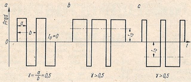
Fig. 1. Rectangular waveforms with different fill factors.
Otherwise, the stage operating in the impulse system can amplify the low frequency vibrations, if we apply a pulse train in which the positive half-period of the low frequency signal is the pulses with the value of γ> 0.5 correspond to the negative half-period, and the pulses with the value of γ <0.5 correspond to the negative half-period (Fig. 2). We are dealing here with pulse width modulation. It goes without saying that the pulse repetition frequency should be much greater than the highest frequency of the amplified low frequency waveform.
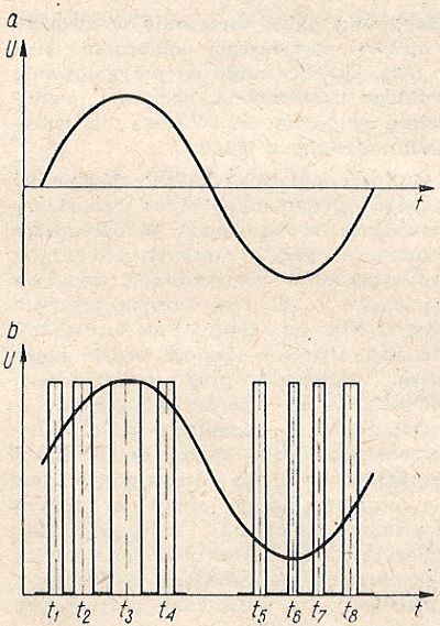
Fig. 2. Pulse width modulation with a sine wave>
a - modulating waveform, b - impulse modulated waveform.
Pulse width modulation can be implemented by various methods. The simplest way is shown in Fig. 3. The triangular voltage is compared with the sinusoidal voltage representing the low frequency signal. Square-shaped pulses appear at the modulator output, the length of which depends on the amplitude of the amplified signal. The triangle waveform can be obtained from square pulses using a Miller integrator.
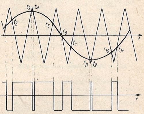
Fig. 3. Pulse width modulation using a triangular voltage.
There are two circuit solutions of class D amplifiers. In the first circuit, the block diagram of which is shown in Fig. 4, an additional generator is used that produces rectangular pulses. After integration in the Miller integrator stage, these pulses are simultaneously supplied with the low-frequency signal to the modulator stage.
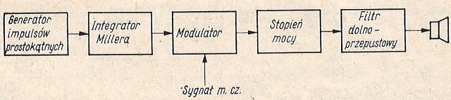
Fig. 4. Block circuit of a class D amplifier with a separate pulse generator.
The second solution does not include an additional rectangular pulse generator. The commutation signal is caused directly by the amplifier with the output coupled to the Miller integrator input. So we have an external feedback circuit, the block diagram of which is shown in Fig. 5.
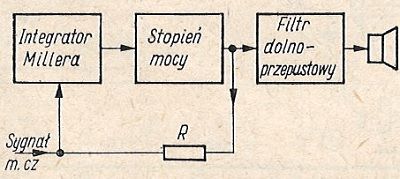
Fig. 5. Block circuit of a class D amplifier without a pulse generator, but with positive feedback.
In both solutions - in order to separate the low frequency signal at the output. - a low-pass filter is required. This filter has a time constant selected to separate RF vibrations. from the highest acoustic frequencies, it is connected in series with the loudspeaker coil.
Practical solutions of class D amplifiers with an output power of 2W
In the diagram of the amplifier presented in Fig. 6, a clear similarity to the block circuit in Fig. 4 can be found. T7 and T8 transistors are part of the astable multivibrator with resistance coupling in the emitter. The multivibrator generates square-wave pulses with a frequency of not less than 50kHz. The vibration frequency depends, among other things, on the capacitance of the C4 capacitor. The duty cycle of the generated pulses should be 0.5 and it is regulated in a small range with a 10kΩ potentiometer in the base circuit of the transistor T8.
Rectangular pulses are fed through the resistor R2 to the base of the transistor T1. This transistor acts as a Miller integrator. It is an amplifier with negative feedback through the capacitor C1. As a result of the Miller effect, the input capacitance at the amplifier input is Cwe - C1 (k + 1), where k - voltage gain of the integrator stage. Thus, an integrator R2Cwe with the time constant τ = R2Cwe = R2C1 (k + 1) is created for rectangular pulses. Thus, the feedback increases the integration time constant (ku + 1) -fold in comparison with the integrating system consisting of the R resistor and the C capacitor. Such a system ensures greater integration accuracy and a higher output voltage. The capacitance of the capacitor C1 is approximately 25pF. At the same time, a low frequency signal is fed to the base of the transistor T1 via the resistor R1. Thus, on the output we get two waveforms: a sinusoidal waveform representing the low frequency signal. and triangular resulting from the integration of rectangular pulses.
The modulator function is performed by the transistor T2, the emitter of which has a constant potential determined by the resistive divider R3 and R4. Rectangular pulses with a width modulated by the low frequency waveform appear at the modulator output. The signal from the modulator controls the amplifier stage with the T3 transistor, working with saturation.
The transformerless output stage with transistors T5 and T6 (complementary pair) is controlled from the emitter follower T4. The emitter potential of the T5 and T6 transistors should be equal to half of the supply voltage. The load on the final stage is the LC low-pass filter and loudspeaker coil.
The gain of the system is increased by the positive feedback loop containing the capacitors C2 and C3. Capacitor C2 increases the blocking efficiency of transistors T4 and T5 during the positive square wave half-cycles. The capacitor C3 improves the blocking certainty of the transistor T6 during the negative half-periods of the square wave.
The frequency characteristic of the amplifier with non-uniformity at the ends of the 3dB band is 20Hz ÷ 10000Hz.
The decrease in the gain at lower frequencies depends mainly on the value of the coupling capacitance, while the decrease in the gain at higher frequencies depends on the reloading rate of the C1 capacitance in the Miller integrator stage, mounting capacities and the inductance value of the low-pass filter.
The output power of the amplifier at a load of 15Ω is 2W.
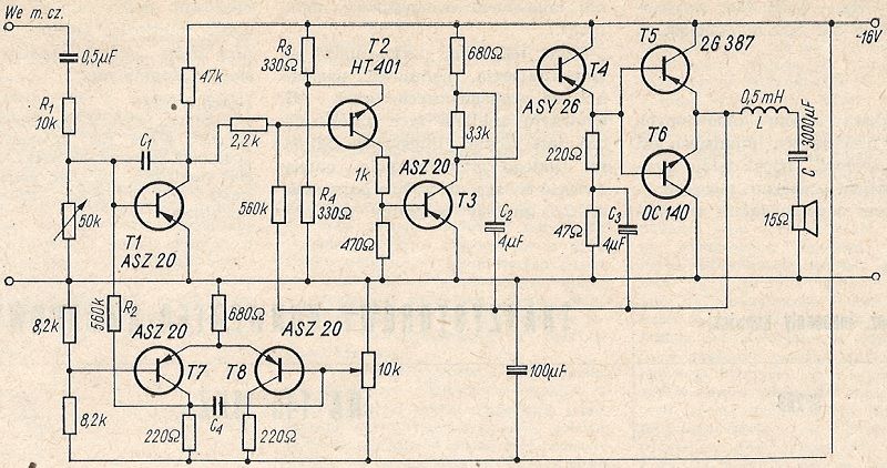
Fig. 6. Diagram of a class D amplifier according to the block layout in Fig. 4.
A more interesting solution is the diagram of an amplifier with external feedback presented in Fig. 7. Coupling the amplifier output with the input of the Miller integrator (through a 560kΩ resistor) allows to obtain, without an additional generator, triangular waveforms used for modulating the width of rectangular pulses. The frequency of vibrations of the set depends on the value of the capacitance C1 and amounts to about 100kHz. Compared to the previous system, the frequency response is much wider and amounts to 20Hz ÷ 20000Hz, -2dB. Output power - 2W on a 15Ω load resistance.
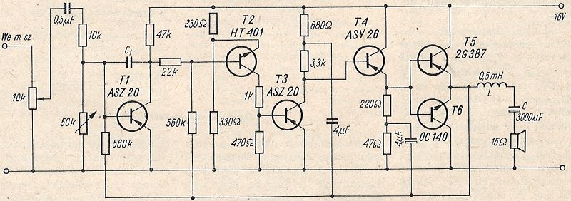
Fig. 7. Schematic diagram of a class D amplifier according to the block layout in Fig. 5.
The greatest advantage of the discussed impulse systems is high efficiency. Thanks to this, it is possible to obtain significant output powers with the use of low power transistors in the final stage. The disadvantage of this type of amplifiers is nonlinear distortion, greater than in class A and B amplifiers. The main source of this distortion is the Miller integrator stage. Therefore, when constructing, attention should be paid to the choice of capacitance C1. Triangular pulses should have a high degree of symmetry and good linearity. The high symmetry of the power stage transistors is also important.
")
")
")
")
")